Environmental chamber - LIB TH-50B
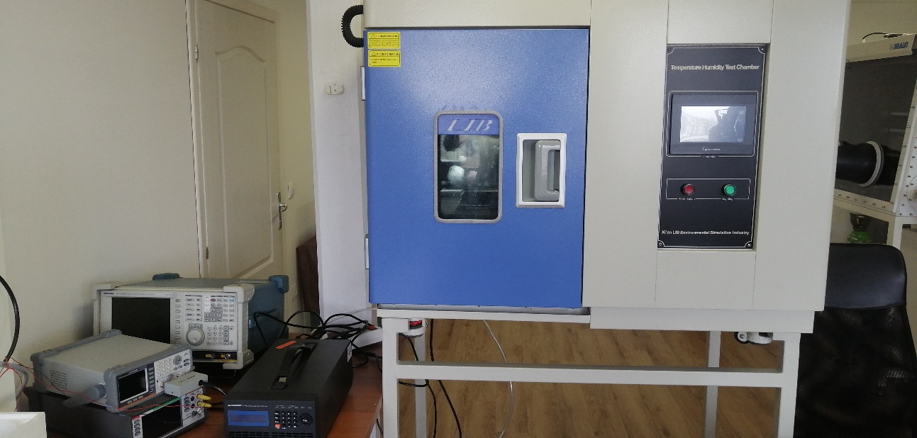
The chamber is intended for environmental control of temperature, humidity and gas atmosphere, for the purpose of testing gas sensors. The volume is 30 liters. The temperature is controlled between -40 and +150 Celsius, with fluctuations not larger than 0.5 degrees. Humidity can be controlled between 20% and 98%, with uniformity of 2.5%. The chamber is controlled from an integrated touchscreen.
The equipment was obtained from funds administered by the Science Fund of the Republic of Serbia, PROMIS program, project Gramulsen (6057070).
Gas concentration control
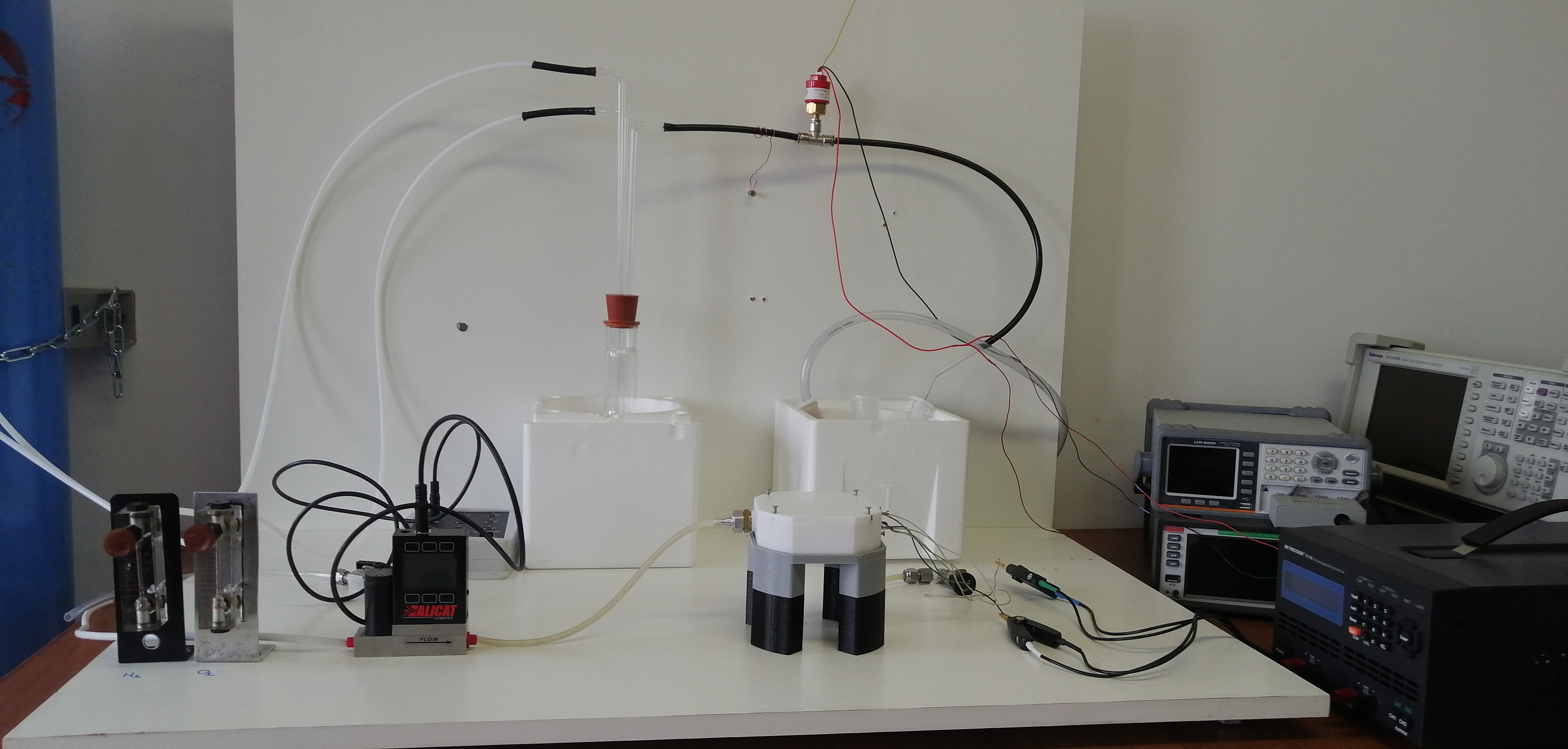
The equipment is used for mixing gases and controlling their concentration in gas chambers. Small volume homebuilt chambers can be used, or the LIB TH-50B. We have two gas control setups in parallel. The first one, relying on glass rotameters for flow control, can elicit concentrations between 0% and 100% with a resolution of ~1%. The second setup relies on mass flow controllers from Alicat, offering the possibility to precisely control gas concentration at levels between 0 and 10,000 ppm.
The equipment was obtained from funds administered by the Science Fund of the Republic of Serbia, PROMIS program, project Gramulsen (6057070), and funds from the Ministry of Education, Science and Technology of the Republic of Serbia.
Laser writer - LW405 (Microtech s.r.l.)
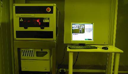
LaserWriter system MICROTECH is intended for writing of planar geometry patterns on photolithographic masks and directly on substrates, as well as for surface diagnostics. It operates with wavelengths down to 0.8 μm and utilizes a gallium nitride laser. The system transforms the laser beam into a controlled tool for direct writing of photolithographic masks and in situ processing of planar substrates (e.g. Si, GaAs, InP, microwave/cryogenic/biological samples, etc). It ensures the fabrication of MEMS structures with submicrometer resolutions. It is convenient for the fabrication of photolithographic masks for small series production, as well as for the fabrication of experimental and prototype microchips. The equipment has been purchased through EU FP7 framework program.
EVG620 Double Side Mask Aligner
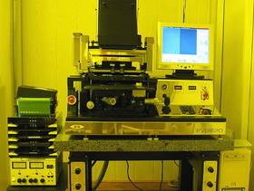
The equipment is used for single or double sided high-resolution photolithography used in planar technology. It allows one to perform highly accurate alignment of patterns on a glass photolithographic mask with the patterns on the substrate (glass, silicon or some other material) with an accuracy better than 1 micrometer. Thus aligned, patterns from the photolithographic mask are transfered to the photosensitive emulsion on the substrate by exposition using UV lamp at 350 nm – 450 nm. The equipment utilizes two microscope, two objectives each, from the top and the bottom side of the substrate to align the patterns. It is equipped by a vacuum and pneumatic system and is fully computer-controlled. The alignment accuracy is 0.06 micrometers. The equipment has been purchased with the help of Serbian Ministry of Science.
Wafer bonder AML-AWB (AML)

The wafer bonding system AWB is a multipurpose system which enables the following types of wafer bonding> adhesive, anodic, direct (high- and low-temperature), eutectic, glass frit, soldering and thermocompression bonding. The equipment enables one to adjust the position of the wafer with an accuracy of 2 to 5 micrometers. A real time control of all its parameters is ensured> current, voltage, temperature, chamber pressure, force, wafer separation, etc. The pressures within the chamber can be adjusted in a range from 10–6 mbar to 2 bar, voltages up to 2.5 kV, temperatures to 560oC and forces to 15 kN. It is possible to bond wafers up to 3" in diameter, as well as semarate microchips. The equipment is especially convenient for the fabrication of complex MEMS systems. The equipment has been purchased through EU FP7 framework program.
Atomic Force Microscope (Thermomicroscopes AutoProbe CP)
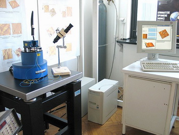
A scanning probe microscope (SPM) for nanometer-resolution characterization of surfaces. Operates as contact AFM (C-AFM), contactless AFM (NC-AFM), Intermittent-Contact AFM (IC-AFM), Lateral Force Microscopy (LFM) and Scanning Tunneling Microscopy (STM). The basic components are the CP-R probe head, the mount with manual XY and automatic Z shift, piezoelectric scanner. The system is equipped with an optical microscope with fiber-optical light source. Maximal sample dimensions 50 mm x 50 mm x 20 mm; measurement range (x, y) plane {90 mm x 90 mm}; z axis to 7,5 mm.
Scanning Probe Microscope Ntegra (NT-MDT)
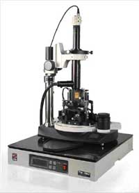
A multifunctional scanning probe microscopy platform that includes atomic force microscopy, but also ensures a possibility to be utilized for scanning near field optical microscopy (SNOM). Enables the use of more than 40 measurement methods. Experiments can be performed in air, vacuum, controlled atmosphere or in liquid. Ensures function at high frequencies, up to 5 MHz. The system performs measures of a wide range of sample sizes, from ultrahigh resolutions at atomic/molecular level up to samples 200x200 µm for X, Y and 22 µm for Z, tje latter being useful for investigation of live tissue and MEMS components. The equipment has been purchased through EU FP7 framework program.
Infrared FTIR spectrophotometer FT-IR 6700 (Thermo Scientific Nicolet)
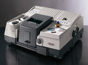
FT-IR 6700 is a Fourier transform infrared spectrophotometer. Ensures measurements in transmission, reflection and attenuated total reflection (ATR) mode. A number of plug-ins is available in the Centre for extension of its function. Operating wavelengths cover the spectrum from NIR to FIR, i.e. 350 cm-1 to 13,500 cm-1 (740 nm to 28.6 μm). FT-IR 6700 utilizes germanium and diamond probes for ATR measurements, which is of importance for characterization of small parts within micro/nanofabricated devices. The system includes specialized software for spectral analysis and processing of measured data. It also ensures automatic removal of the influence of atmosphere (water, carbon dioxide) and photoacoustic method. The equipment has been purchased through EU FP7 framework program.
Infrared microscope and FTIR spectrophotometer iN10 (Thermo Scientific Nicolet)
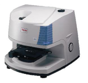
Infrared microscope and FTIR spectrophotometer iN10 FT-IR measurements in transmission, reflection and attenuated total reflection (ATR) mode at micrscopic samples. The measurement location is chosen using a CCD camera and a visible range microscope, and IR spectres are measured from areas with the dimensions down to 50 μm x 50 μm. The system includes software for picture sampling and spectral analysis. The equipment has been purchased through EU FP7 framework program.
Silicon Oxidation/diffusion Furnace Helmut Seier gmbh
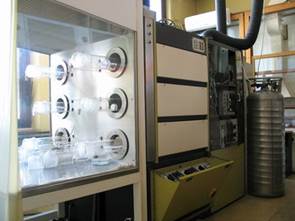
A furnace with a horizontal 3-stack configuration, used in CMT for doping of silicon wafers (2" i 3”) with p-tipa (boron) and n-type dopants (phosphorous), as well as for forming of high-quality thermal oxide (wet and dry oxidation). Operating temperatures 800-1200oC, thermal regulation zone with an accuracy of ±0.5oC; the zone width of about 10 cm. Contains a system for introduction of carrier gases and a system for humidity control.
Sputtering system Perkin Elmer 2400
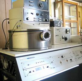
A sputtering system for semiconductor processing, designed to ensure high frexibility in the choice of targets (cathode diameter 6”) and operating modes. CMT utilizes a number of different cathodes> metals and their alloys, semiconductors, oxides. Operating modes include RF/DC sputtering, RF etching and reactive sputtering. To attain high vacuum (below 10-6 mbar) the system is equiped by a mechanical and turbomolecular pump (Leybold TURBOVAC 361) with a digital controler. Sputtering with rotation of support carrying substrate samples ensures simultaneous processing of a larger number of substrates (the number depends on their diameter – maximum 20 cm) but also ensures a better uniformity of the deposited film.
Automatic prober KARL SUSS AP4
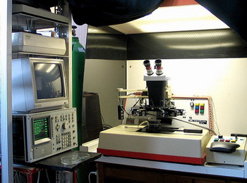
The equipment is intended for automatic and manual measurement and characterization of semiconductor devices at an area of up to 100 mm in diameter. It simultaneously performs measurements in 42 points, which ensures the possibility to measure more complex components including integrated circuits. It is equipped with a stereoscopic microscope with zoom. It ensures automatic movement in x and y direction with a minimum step of 10 µm.
