
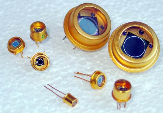
We produce PIN photodiodes on n-type and p-type substrate, standard and quadrant, with active areas from 0.8 mm2 to 80 mm2 (other sizes on request).
n-type Photodiodes
Our n-type silicon PIN photodiodes are optimized for detection of radiation at 900 nm. A photodiode illuminated by visible and near infrared light behaves as a current source with photocurrent proportional to the power of detected radiation. Reverse bias increases parallel internal resistance and decreases capacity of diode. Decrease of capacity and of load resistance RL decreases response time. Low capacity with relatively low bias is achieved by using extremely pure, high resistance silicon for the base I-region of the diode (> 2 kΩcm). Background radiation flux increases noise current, thus filters or darkening are recommanded to decrease this radiation.
| FD08N | FD5N FD5N1 |
FD80N | ||
| Type |
N | N | N | |
| Active area (mm2) | 0.8 | 5 | 80 | |
| Housing | TO-18 | TO-5 | TO-25 | |
| Supply voltage (V) | 45 | 45 | 45 | |
| Breakdown voltage (V) | 100 | 100 | 100 | |
| Dark current (nA) | typical | 2 | 20 | 50 |
| max | 20 | 50 | 300 | |
| Responsivity (A/W) | 900 nm typical | 0.60 | 0.60 | 0.60 |
| 900 nm min. | 0.50 | 0.50 | 0.50 | |
| 1060 nm typical | 0.15 | 0.15 | 0.15 | |
| 1060 nm min. | 0.10 | 0.10 | 0.10 | |
| NEP (10-12Hz1/2) | 900 nm typical | <1 | <1.5 | 5 |
| 900 nm max | 5 | 7 | 20 | |
| 1060 nm typical | <4 | <4 | 20 | |
| 1060 nm max | 20 | 20 | 80 | |
| Capacity (pF) | typical | 2.5 | 8 | 70 |
| max | 3 | 10 | 120 | |
| Response (ns) | 900 nm | 3.11) | 51) | 101) |
1) at 50% of amplitude
Download pdf versions of data sheets for our n-type diodes:
n-type Si PIN diode, active area 0.8 mm2
n-type Si PIN diode, active area 5 mm2, standard height or with a low-cap housing
n-type Si PIN diode, active area 80 mm2
p-type Photodiodes
Our p-type silicon PIN photodiodes are optimized for detection of radiation at 1060 nm. A photodiode illuminated by visible and near infrared light behaves as a current source with photocurrent proportional to the power of detected radiation. Reverse bias increases parallel internal resistance and capacity of diode. Decrease of capacity and of load resistance RL decreases response time. Low capacity with relatively low bias is achieved by using extremely pure, high resistance silicon for the base I-region of the diode (> 10 kΩcm). Background radiation flux increases noise current, thus filters or darkening are recommanded to decrease this radiation. Influences of transition area width and cross-talk influence are minimized for our quadrant-type PIN diodes.
| FD5P FD5P1 |
QDY7P 3) | QDY80P 3) | ||
| Type | P | P | P | |
| Active area (mm2) | 5 | 7 | 80 | |
| Housing | TO-5 | TO-5, 8 | TO-25 | |
| Supply voltage (V) | 200 | 200 | 200 | |
| Breakdown voltage (V) | 250 | 250 | 250 | |
| Dark current (nA) |
typical | 20 | 10 | 100 |
| max | 100 | 50 | 1000 | |
| Responsivity (A/W) | 900 nm typical | 0.60 | 0.60 | 0.60 |
| 900 nm min. | 0.50 | 0.50 | 0.50 | |
| 1060 nm typical | 0.45 | 0.45 | 0.45 | |
| 1060 nm min. | 0.40 | 0.40 | 0.40 | |
| NEP (10-12Hz1/2) | 900 nm typical | <1.5 | <1.5 | 5 |
| 900 nm max | 10 | 7 | 40 | |
| 1060 nm typical | <2.5 | <2.5 | 7 | |
| 1060 nm max. | 15 | 12 | 60 | |
| Capacity (pF) | typical | 2.5 | 1.2 | 7 |
| max | 3 | 1.4 | 10 | |
| Response (ns) | 900 nm | <112) | <112) | <201) |
2) 10% - 90% of amplitude
3) per quadrant
Download pdf versions of data sheets for our p-type diodes:
p-type Si PIN diode, active area 5 mm2, standard height or with a low-cap housing
quadrant p -type Si PIN diode, active area 7 mm2
quadrant p -type Si PIN diode, active area 80 mm2


